

For more than a decade, atomically thin semiconductors have stood out as a promising route beyond conventional silicon. These materials can be just a single atom thick while still offering impressive electrical properties. In principle, they could enable transistors that are smaller, faster, and more energy efficient than today’s devices. Yet even as researchers have discovered increasingly capable two-dimensional semiconductor materials, one stubborn engineering problem has remained.
A working transistor requires an extremely thin insulating layer known as the gate dielectric. This layer sits above the semiconductor and helps control the movement of electrons. As transistors shrink, making this insulating layer thinner can improve electrical control. The difficulty is that adding such layers to atomically thin semiconductors can disturb the delicate interface between the materials. That disruption can scatter electrons and erase some of the performance gains engineers are trying to achieve.
For years, researchers have therefore faced a difficult tradeoff. They could strengthen control over the transistor gate, or they could protect the mobility of the charge carriers moving through the device. Achieving both at once has been much harder.
A New Strategy for Atomically Thin Transistors
Researchers at National Yang Ming Chiao Tung University (NYCU), working with TSMC Corporate Research, have now demonstrated a new way to address this problem by focusing on the interface itself.
The work, published in Nature Electronics, shows that carefully controlling the atomic boundary between a semiconductor and its insulating layer can allow the dielectric to be made extremely thin while maintaining strong electrical performance. Rather than searching for a completely different semiconductor, the researchers concentrated on the narrow region where the two materials meet, an area only a few atoms thick.
“For many years, efforts to improve atomically thin transistors have largely focused on discovering better semiconductor materials,” said Professor Wen-Hao Chang, the study’s corresponding author from NYCU. “Our research shows that the atomic interface between materials can be just as important. By engineering that boundary, we were able to reduce one of the fundamental trade-offs that has limited two-dimensional transistors for many years.”
Why the Atomic Interface Matters
Modern chip development depends heavily on shrinking transistor components. One of the most important is the gate dielectric, which electrically separates the gate electrode from the transistor channel.
Silicon technology has benefited from decades of refinement, allowing manufacturers to produce dielectric materials capable of controlling progressively smaller devices. Atomically thin semiconductors, however, behave differently. Their surfaces do not contain dangling bonds, which makes it difficult to grow an extremely thin dielectric film evenly across them.
Standard deposition techniques can leave gaps, create defects at the interface, and introduce electrical disorder. These problems can reduce carrier mobility and weaken transistor performance.
Researchers around the world have explored several possible solutions, including different dielectric materials, molecular seed layers, and alternative methods for depositing oxides. Although these approaches have produced significant improvements, it remains difficult to achieve low equivalent oxide thickness, strong electrostatic control, and high carrier mobility at the same time. The challenge is especially significant in wafer-scale CVD-grown monolayer MoS2.
Building a Buffer Only a Fraction of a Nanometer Thick
Instead of changing either the semiconductor or the gate dielectric, the NYCU researchers redesigned the interface connecting them.
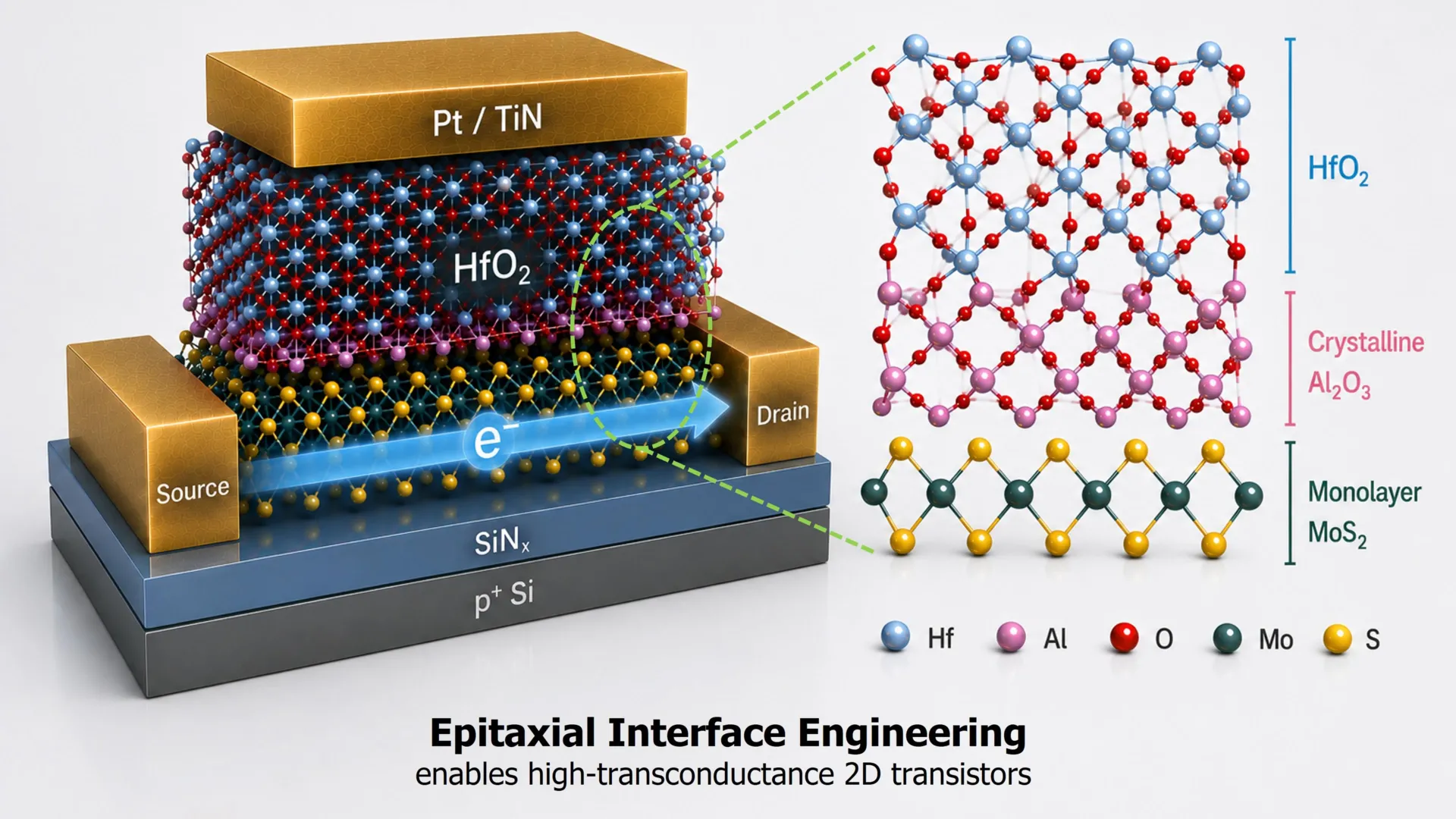
The team first placed an ultrathin epitaxial aluminum layer directly onto monolayer molybdenum disulfide (MoS2). They then carefully oxidized the aluminum, producing an aluminum oxide layer about 0.42 nanometers thick. After that, they added the high κ hafnium oxide gate dielectric.
Despite being only a fraction of a nanometer thick, the engineered interface performs two important jobs.
First, it creates a smooth and continuous surface that allows the hafnium oxide to grow more uniformly over the MoS2. Second, it works as an atomic buffer that limits unwanted electrical interactions between the dielectric and the semiconductor. This protection helps electrons continue moving efficiently through the transistor channel.
In this design, the interface does more than simply keep two materials apart. It becomes a functional part of the transistor and helps the materials work together more effectively.
Combining Thin Dielectrics With Strong Performance
Using the new interface design, the researchers fabricated short-channel top-gate transistors from CVD-grown monolayer MoS2. The devices had an equivalent oxide thickness of roughly one nanometer.
Testing showed low leakage current, minimal hysteresis, and maximum transconductance of 0.45 mS μm-1 in transistors with channels measuring about 100 nanometers.
More importantly, the devices demonstrated a combination that has been difficult to achieve in atomically thin transistors: very thin dielectric scaling, strong electrostatic control, and sustained carrier transport.
Because the researchers used CVD-grown monolayer MoS2 rather than mechanically exfoliated flakes, they believe the approach brings the technology closer to materials and processes that could eventually be suitable for wafer-scale manufacturing.
Rethinking How Future Chips Are Designed
The findings also point to a broader change in the way semiconductor researchers think about transistor design.
For decades, much of the effort to improve transistors has centered on discovering better semiconductor materials or making devices smaller. As transistor components approach atomic dimensions, however, the interfaces separating different materials become increasingly important.
These regions may be only a few atoms thick, yet they can strongly influence how well the materials on either side work together. The new results add to growing evidence that controlling these atomic interfaces could become as important as developing new semiconductor materials themselves.
“When transistor components become only a few atomic layers thick, the interface is no longer simply the boundary between materials, it becomes an active part of the device,” said Professor Tsung-En Lee, the study’s corresponding author. “Learning to engineer these interfaces with atomic precision opens new opportunities for designing future semiconductor devices that would be difficult to achieve by changing individual materials alone.”
A Possible Route Beyond Silicon
As the semiconductor industry looks for ways to continue improving chips beyond traditional silicon scaling, atomically thin materials are receiving growing attention for future low-power logic and advanced electronic systems.
More work will still be needed before the fabrication process can be optimized for large-scale manufacturing. Even so, the researchers view their interface engineering method as an important step toward practical two-dimensional electronics.
The findings suggest that future semiconductor advances may depend not only on discovering new materials, but also on learning how to precisely control the atomic boundaries that connect them. As transistors shrink toward the dimensions of individual atoms, those interfaces could become some of the most important parts of the devices themselves.