

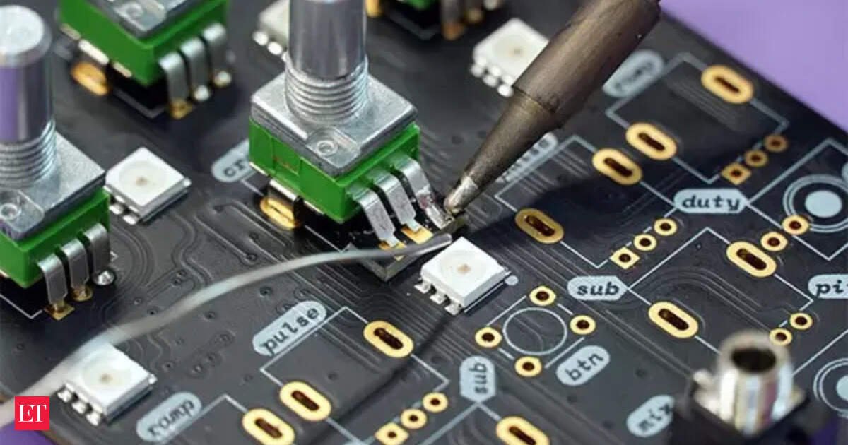
The semiconductor package, approved with a budgetary outlay of Rs 1,27,500 crore, builds on the momentum of Semicon 1.0 and seeks to further the government’s commitment to putting India on the global semiconductor map by strengthening the country’s semiconductor design and manufacturing ecosystem.
Also read: Cabinet highlights: India clears Rs 2.19 lakh crore mega push across chips, corridors and mobile manufacturing
Announcing the decisions after a meeting of the Union Cabinet and the Cabinet Committee on Economic Affairs (CCEA), Electronics and Information Technology Minister Ashwini Vaishnaw said the semiconductor package was among seven major decisions cleared under the prime minister’s chairmanship.
“I am presenting before you the seven major decisions taken by the Cabinet and the Cabinet Committee on Economic Affairs (CCEA) under the chairmanship of Prime Minister Narendra Modi. The first two decisions relate to a programme for developing infrastructure in Varanasi (Kashi) in a completely new way. The third, fourth, and fifth decisions relate to the Semicon 2.0 Mission (Semiconductor 2.0 Mission), which was approved today,” Vaishnaw said.

Vaishnaw also announced the approval of the Rs 62,500-crore Mobile Phone Manufacturing Scheme (MPMS) as part of the Cabinet decisions.
“The fourth decision is the approval of the Mobile Phone Manufacturing Scheme. The fifth decision is aimed at making India self-reliant in urea, for which the National Investment Policy for Urea was approved today. The sixth and seventh decisions relate to proposals for the upgradation of the railway network, including track doubling and the construction of a fourth railway line,” the Union Minister said.The approvals formed part of a broader package of seven Cabinet decisions worth about Rs 2.19 lakh crore, which also included infrastructure projects in Varanasi, the National Investment Policy for Urea-2026, the doubling of the Paradeep-Haridaspur railway line, and the construction of a fourth railway line between Dangoaposi and Rajkharsawan.
Also read: Cabinet approves Rs 62,500 crore for mobile phone PLI scheme 2.0
Semicon 2.0: Six-pillar roadmap
The government said Semicon 2.0 has been designed as a long-term programme to strengthen India’s semiconductor ecosystem by building capabilities across the entire value chain while carrying forward the momentum generated under Semicon 1.0.
The first pillar focuses on chip design, with the government aiming to deepen the domestic design ecosystem after 105 startups began developing chips under the earlier programme. Under Semicon 2.0, the focus will be on developing semiconductor intellectual property (IP), chip designs and systems, with the objective of positioning India as a leading semiconductor design IP country.
The second pillar targets machines and materials by incentivising companies engaged in the manufacturing and research and development of semiconductor equipment, as well as the materials, chemicals and gases essential for chip production. According to the government, this is expected to support the long-term growth of the semiconductor industry while strengthening India’s precision manufacturing capabilities.
The third pillar seeks to attract more semiconductor fabrication units to India. With the country’s first fab scheduled to be commissioned in 2028, the government plans to encourage investments across silicon fabs, compound semiconductor fabs, discrete component fabs and display fabs.
The fourth pillar focuses on further strengthening the Assembly, Testing, Marking and Packaging (ATMP) and Outsourced Semiconductor Assembly and Test (OSAT) industry by encouraging more advanced packaging technologies and facilities as global companies increasingly view India as an alternative manufacturing destination.
The fifth pillar centres on research and development, with the government planning to move beyond the current 28nm-110nm technology nodes towards more advanced semiconductor technologies through collaboration with leading R&D centres within and outside India.
The sixth pillar focuses on talent development. The government said 315 universities are already training students in complex chip design using industry-standard Electronic Design Automation (EDA) tools, with around 68,000 students trained so far. The programme aims to deepen this training while increasing industry participation in clean room operations, fab construction and other specialised semiconductor ecosystem skills.
Progress under Semicon 1.0
The government said Semicon 2.0 builds on the progress achieved under the first phase of the India Semiconductor Mission, under which 12 manufacturing units with a cumulative investment of over Rs 1.64 lakh crore have been approved.
These include one silicon fab, one silicon carbide fab, an integrated gallium nitride Micro LED display fab and nine semiconductor packaging units that are expected to cater to sectors including consumer appliances, industrial electronics, automobiles, power electronics, telecommunications and aerospace.
Of the 12 approved manufacturing projects, Micron, Kaynes and CG Semi have already started commercial production, while another manufacturing unit is expected to begin operations in 2026.
On the design front, 24 semiconductor design projects from startups and MSMEs have been approved for financial support, while 105 startups and MSMEs have been granted access to industry-standard Electronic Design Automation (EDA) tools. These firms are designing chips and systems-on-chip (SoCs) for applications including satellite communications, drones, surveillance cameras, Internet of Things (IoT) devices, LED drivers, artificial intelligence systems, telecom equipment and smart meters, with deployment expected after successful prototyping.